教員・研究員紹介
- 松田 時宜 (まつだ ときよし)
- 教授 博士(理学)
- 所属学科/電気電子通信工学科 所属専攻/エレクトロニクス系工学専攻
- 研究キーワード:
- 数値シミュレーション/半導体/ナノ材料/ナノ構造制御/材料開発/バッテリー開発/ナノ科学・ナノテクノロジー/電気電子材料工学/低次元物質/半導体工学/パワーエレクトロニクス/人工知能/機械材料/材料プロセス工学/センサー工学/ナノエレクトロニクス/半導体製造プロセス/ディスプレイ/熱電変換/プラズマ応用/シミュレーション/ナノ粒子/環境分析/グリーンプロセス/電子デバイス物理学/機能材料化学/元素戦略/基礎電子デバイス物理学/電池/高電圧プラズマ物理・工学/結晶/グリーンケミストリー/セラミックス/センサー/バイオセンサー/マテリアルサイエンス/高電圧・プラズマ工学/シミュレーション工学/半導体デバイス/パワーデバイス/プロセスインフォマティクス/薄膜/電子材料
酸化物半導体を中心として、新しいセンシングデバイス、MEMSを提案していきます。
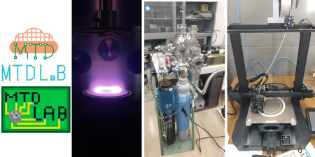
| 専門 | センサー, MEMS, 酸化物半導体材料 |
|---|---|
| 担当科目(学部) | 近大ゼミ1, 近大ゼミ2, 電気電子通信工学概論, 電気計測, 半導体工学, 科学術英語2, センサ工学,メカトロニクス, 卒研ゼミナール, 卒業研究 |
| 担当科目(大学院) | 機能性デバイス特論, エレクトロニクス系工学特別研究, 機能性デバイス特殊研究 |
| 主な研究テーマ | センサー, MEMS, デバイス作製プロセス |
| 代表的な研究業績 |
1.Matsuda, T., Umeda, K., Kato, Y., Nishimoto, D., and Kimura, M., Rare-metal-free high-performance Ga-Sn-O thin film transistor, Scientific Reports, (2017), 7, 44326 2.Sugisaki, S., Matsuda, T., Uenuma, M., Nabatame, T., Nakashima, Y., Imai, T., Magari, Y., Koretomo, D., Furuta, M., and Kimura, M., In-Ga-Zn-O Thin-film Devices as Synapse Elements in a Neural Network, Scientific. Reports. (2019), 9, 2757. 3.Matsuda, T., and Kimura, M., Comparison of defects in crystalline oxide semiconductor materials by electron spin resonance Journal of Vacuum Science and Technology A Letters, Vol. 33, (2015), No. 2, 020601. 4.Matsuda, T., Furuta, M., Hiramatsu, T., Furuta, H., Kawaharamura, T., and Hirao, T. Low Temperature Deposition of SiOx Film with Newly Developed Facing Electrodes Chemical Vapor Deposition, Vacuum, 101 (2014), 189-192. 5.SID2006、Distinguished Paper Award受賞関連論文 Hirao, T., Furuta, M., Furuta, H., Matsuda, T., Hiramatsu, T., Hokari, H., Yoshida, M., Ishii, H., and Kakegawa, M., Novel top-gate zinc oxide thin-film transistors (ZnO TFTs) for AMLCDs Journal of Society for Information Display, Vol. 15, Issue 1, (2007), 17-22. |
| 研究内容・研究成果 | |
| researchmap | https://researchmap.jp/toki |
| 所属学協会 | 応用物理学会 IEEE |
| 学外活動 | AM-FPD IEEE EDS Kansai Chapter |
| 出身大学 | 大阪大学 理学部 物理学科 |
| 出身大学院 | 大阪大学大学院理学研究科 宇宙地球科学専攻 |
| 論文名、取得大学、取得年月 | Adsorption of gas and heavy metal ions on clay minerals and hydroxyapatite 博士(理学) 大阪大学 (17569号)、2003年3月25日 大阪大学 |
| 主な経歴 | 2003年ブラジルサンパウロ州立大学 博士研究員,2004年 高知工科大学 助教,2011年 龍谷大学 助教,2017年 株式会社 FLOSFIA |
| 受賞歴 | Distinguished Contributed Paper Award, SID2006 Poster Paper Award (Co-author) Low-Temperature Synthesis of SiO2 Insulator by ICP-CVD Using Tetramethylsilane 13th International Display Workshops 06 (IDW06) 15 th place Top 20 Most Downloaded Articles, January 2010 Crystallinity and Resistivity of ZnO thin films with indium implantation and post annealing Journal of Vacuum Science and Technology, A ベストペーパーアワード(発表者) ZnO薄膜蛍光体の形成と発光中心導入過程 薄膜材料デバイス研究会 Best Paper Award (Presenter) Fabrication of ZnO thin film phosphor and induced luminescence center Thin Film Materials and Devices Meeting (Japanese) 丹羽高柳賞「論文賞」 (共著者として) 有機光導電膜とZnO TFT回路の積層構造を用いた有機撮像デバイスの原理実証実験 社団法人 映像情報メディア学会 |
| 学生へのアドバイス | 学生時代は人生の中で世界が大きく広がる期間です。今現在だけでなく,将来の自分自身にとって大事なことを見極められるような価値観を得られる経験をしてください。 |
| 学生に薦めたい書物 | (1)安宅 和人 イシューからはじめよ 知的生産の「シンプルな本質」 英治出版 2010 (2)星野 達也 オープン・イノベーションの教科書 ダイヤモンド社 2015 (3)アンドリュー・S・グローブ HIGH OUTPUT MANAGEMENT 日経BP 2017 (4)田端 信太郎 これからの会社員の教科書 SBクリエイティブ 2019 |
| 趣味・その他 | 最近アウトドアにはまりつつあります |
機能性デバイス研究室
| 教員室 | 31号館7階 松田教授室 |
|---|---|
| 内線 | 4318 |
| メールアドレス | matsuda(at)ele.kindai.ac.jp
|