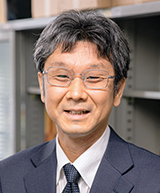
Researchers

- KANASHIMA Takeshi
- Professor/Manager
| Faculty | Department of Electric and Electronic Engineering / Graduate School of Humanity-Oriented Science and Engineering |
|---|---|
| Researchmap | https://researchmap.jp/read0046497 |
Education and Career
Education
- 1987/04 - 1991/03 , Osaka University, Faculty of Engineering Science,
- 1991/04 - 1993/03 , Osaka University, Graduate School of Engineering Science,
- 1993/04 - 1996/03 , Osaka University, Graduate School of Engineering Science,
Academic & Professional Experience
- Apr. 2022 - Today , Kindai University Faculty of Humanity-Oriented Science and Engineering Department of Electric and Electronic Engineering Professor
- Jul. 2007 - Mar. 2022 , Osaka University Graduate School of Engineering Science 准教授
- Apr. 2007 - Jun. 2007 , Osaka University Graduate School of Engineering Science 助教
- Apr. 1996 - Mar. 2007 , Osaka University Faculty of Engineering Science 助手
Research Activities
Research Areas
- Manufacturing technology (mechanical, electrical/electronic, chemical engineering), Electric/electronic material engineering
- Nanotechnology/Materials, Thin-film surfaces and interfaces
Research Interests
high-Kゲート, 放射光による電子材料の作製及びエッチング, Si/SiO界面の評価, Si酸化膜, high-K gate., Preparation and Etching of Electrical Materials by Synchro-Radiation, characterization of SiO<sub>2</sub> thin fims and Si/SiO<sub>2</sub> interface
Published Papers
-
Metastable Co3Mn/Fe/Pb(Mg1/3Nb2/3)O3–PbTiO3 multiferroic heterostructures
Y. Murakami; T. Usami; R. Watarai; Y. Shiratsuchi; T. Kanashima; R. Nakatani; Y. Gohda; K. Hamaya
Journal of Applied Physics 134 (22) 8, Dec. 2023 -
Converse magnetoelectric coupling coefficient greater than 10^{-6} s/m in perpendicularly magnetized Co/Pd multilayers on Pb(Mg_{1/3}Nb_{2/3})O_{3}-PbTiO_{3}
T. Usami; Y. Sanada; Y. Shiratsuchi; S. Yamada; T. Kanashima; R. Nakatani; K. Hamaya
Journal of Magnetism and Magnetic Materials 570 (15) , 170532-170532, Mar. 2023 , Refereed -
Giant converse magnetoelectric effect in a multiferroic heterostructure with polycrystalline Co2FeSi
Shumpei Fujii; Takamasa Usami; Yu Shiratsuchi; Adam M. Kerrigan; Amran Mahfudh Yatmeidhy; Shinya Yamada; Takeshi Kanashima; Ryoichi Nakatani; Vlado K. Lazarov; Tamio Oguchi; Yoshihiro Gohda; Kohei Hamaya
NPG Asia Materials 14 (1) Dec. 2022
Books etc
- P(VDF-TeFE)/Organic Semiconductor Structure Ferroelectric-GateFETs , T. Kanashima; M. Okuyama , Springer , Jan. 2016
MISC
- Converse magnetoelectric effect in Co-based Heusler alloy/PMN-PT(011) multiferroic heterostructures , USAMI Takamasa; FUJII Shumpei; YATMEIDHY Amran Mahfudh; GOHDA Yoshihiro; GOHDA Yoshihiro; OKABAYASHI Jun; YAMADA Shinya; YAMADA Shinya; KANASHIMA Takeshi; SHIRATSUCHI Yu; SHIRATSUCHI Yu; NAKATANI Ryoichi; NAKATANI Ryoichi; HAMAYA Kohei; HAMAYA Kohei , 応用物理学会春季学術講演会講演予稿集(CD-ROM) , 69th , 2022
- Wet treatment effects to the contact angle of Ge surface and the relations to electrical properties of MIS structure , 高山祐太郎; 森悠; 金島岳 , 応用物理学会春季学術講演会講演予稿集(CD-ROM) , 67th , 2020
- Etching of Ge substrate surface by iodine solution treatment , 森悠; 濱地威明; 阿保智; 酒井朗; 金島岳 , 応用物理学会秋季学術講演会講演予稿集(CD-ROM) , 81st , 2020
Patents
- 強誘電体メモリ及びその製造方法
Awards & Honors
- 2006, JJAP論文賞
Research Grants & Projects
- Japan Society for the Promotion of Science, Grants-in-Aid for Scientific Research, High quality Ge-based transistor using epitaxially grown high-k gate insulators , Osaka University
- Japan Society for the Promotion of Science, Grants-in-Aid for Scientific Research, Preparation of Ferromagnetic and Ferroelectric Thin Films by Pulsed Laser Deposition and Their Characterization , Osaka University
- Japan Society for the Promotion of Science, Grants-in-Aid for Scientific Research, Improvement of insulator/ Germanium interface by surface passivation for high-mobility Ge based transistor. , Osaka University